My project student selalu tanya macam mana nak guna developer and etching printed circuit board (PCB). The things is they all malas nak mencari. Tak tahu la nak marah cam mana lagi. So students out there yang tengah membaca ni, rajin2 juga la buka website yang berilmiah skit untuk upgrade diri kita yang lemah ini.
So, I would like to share cara2 untuk expose, developer and etching.
------------------------------------------------------------------------------------------------------------
Today, i decided to make PCB board using UV (Ultra Violet) method for sharing the knowledge on the procedures & process of UV PCB construction. Here are some of pictures with brief explanation.
Step 1: Print a circuit on laminate paper
Step 2: Buy a Kinsten Coated PCB - GS1015 for single layer and the manual instruction inside the product.
Step 3: Attach a circuit together with Kinsten Coated PCB and expose it with light (photoresis) using UV machine around 90 to 120 second.
Step 4 : A picture of PCB after photoresis process. Remove a circuit from PCB and you can use again the same laminate for other PCB.
Step 5 : Quickly bath a circuit with water and developer then shake it until the unwanted layer remove from the PCB.
Figure A : Picture sample of developer. You can used other product you like.
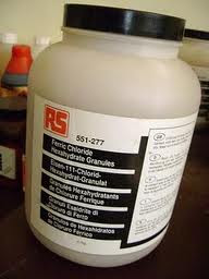
Step 6 : After wash a PCB, bath the PCB with ferrite chloride & hot water then shake the PCB again until the second unwanted layer removed from the PCB.
Figure B : Picture sample of ferrite chloride product. Caution! You are deal with dangerous chemical (developer & ferrite chloride). Wash you hand after using it. Please use a glove if possible and dispose the chemical properly.
Step 7 : Lastly, brush your circuit and see the different. Now, you can cut any PCB size and drill the PCB for soldering purpose. That's all :)
(credit to 9m2esm.blogspot.com)


